Week 08: Electronics Desing
Components of circuits
This week, we're starting to learn about various components of circuits:
Resistors
Resistors are very important components of circuits. They are passive components that regulate the flow of current (limit, divide voltage, measure current). Resistors can have different degrees of resistance in a circuit. The degree of resistance is indicated in ohms. You can identify the degree of resistance by the color bands on the resistor. Resistors used for SMD cards can also be distinguished by printed numbers. The safest way to determine the resistance is to measure it with a multimeter.
Voltage Divider
A voltage divider is an electronic circuit used to divide an input voltage into two or more output voltages. This circuit typically consists of two resistors connected in series. The output voltages depend on the resistance values and the ratio of the resistors to each other. Voltage dividers are used in various applications to reduce voltage, set a reference point, or adjust signals.
Pull-up Resistor
A pull-up resistor is an electrical resistor used to pull an input to a specific voltage level, usually logically "high" when no active signal is present. It stabilizes the state of the line and prevents unwanted signals.
Capacitors
Capacitors are electronic components capable of storing and releasing electric charge. They consist of two conductors separated by an insulating material, also called a dielectric. There are polarized and non-polarized capacitors (I can use non-polarized ones as I wish). Capacitors ensure that the voltage remains constant. They are like small batteries that can hold the voltage.
Diode
A diode is an electronic component that allows electric current to pass in one direction and blocks the flow of current in the opposite direction. It functions like an electrical valve, allowing current flow in only one direction. LEDs are diodes. The flow of current can also be blocked through them since the current flows in only one direction.
Zener Diodes
Zener diodes are diodes that, for example, block the flow of current above a certain voltage.
Schottky Diodes
Schottky diodes are a special type of semiconductor diodes characterized by their fast switching speed and low forward voltage. Compared to conventional silicon diodes, Schottky diodes have a metal-semiconductor junction instead of a p-n junction. This results in faster response and lower power loss. Schottky diodes are commonly used in high-frequency applications, power amplifiers, rectifiers, and other circuits requiring high power and fast switching speed.
Oscillator
The main function of an oscillator is to generate a stable and recurring signal, typically used as a clock signal or reference signal for other circuits in electronic devices. This clock signal is often fundamental for the operation of digital circuits, microcontrollers, radios, clocks, and many other electronic devices.
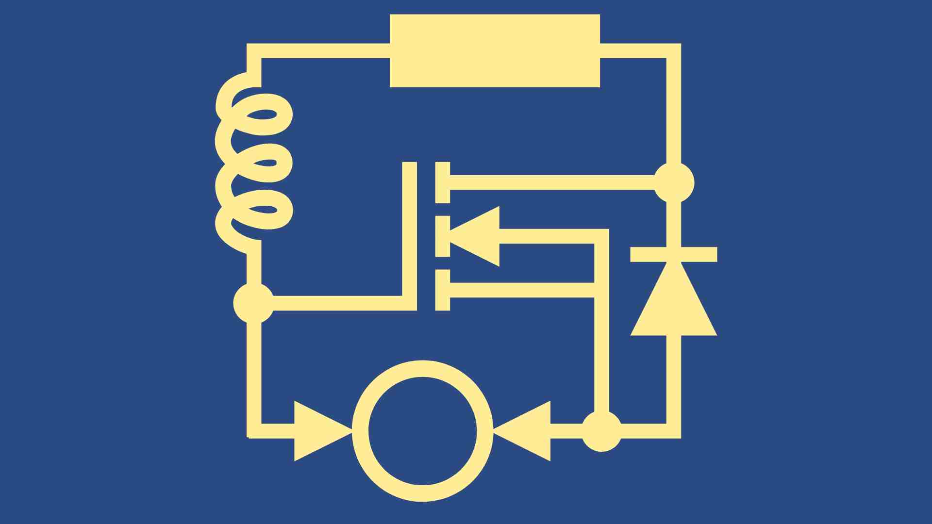
Transistors
A transistor is essentially like a tiny switch in electronic devices. It controls the flow of current (like a faucet controls the flow of water), which is used in many devices such as computers, mobile phones, and televisions to control and operate them.
MOSFET (we will use this a a transistor)
The MOSFET operates similarly to a regular transistor, but it has special properties that make it more efficient. It is often used in circuits to control the flow of current. MOSFETs are used in many devices, from computers to solar cells, because they can regulate current well and consume little energy.
Regulator
A regulator is used to ensure a constant output voltage or current, regardless of fluctuations in input voltage or other external conditions. A regulator works like a stabilizer: it ensures that the energy coming from the battery remains at a constant level, so that the connected devices are always supplied with a stable and safe power source.
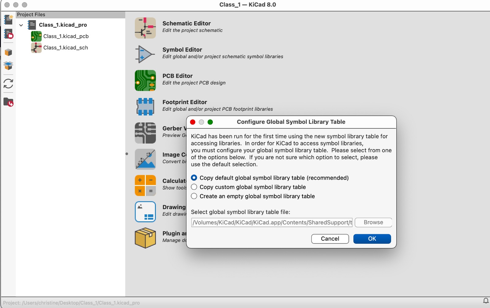
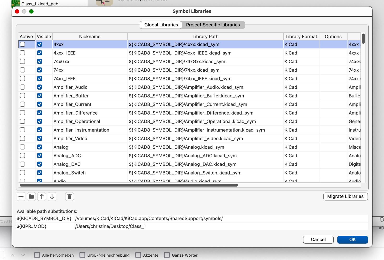
KiCad
There are many different programs for PCB design. We choose KiCad because it is a very good open-source software. It is updated annually, and we are working with the latest version. We can produce our drawings ourselves or send them for production. However, we can also print the drawings we produce ourselves.
In KiCad, there are various workbenches:
- Schematic Editor: This workspace allows you to design electronic schematics. Here, components can be added, connected, and electrical connections can be created.
- PCB Layout Editor: Here, the layout of the PCB can be created, determining the positioning and connection of components on the PCB. Components can be placed, and traces can be routed.
- Footprint Editor: Here, footprints for individual components can be created. Footprints are important for later positioning the components on the PCB.
- Symbol Editor: Individual symbols for electronic components can be created, and existing symbols can be adjusted.
- 3D Viewer: The 3D viewer allows you to preview the PCB in 3D, to see how the components are physically placed on the PCB. This helps to verify if the PCB can function as intended.
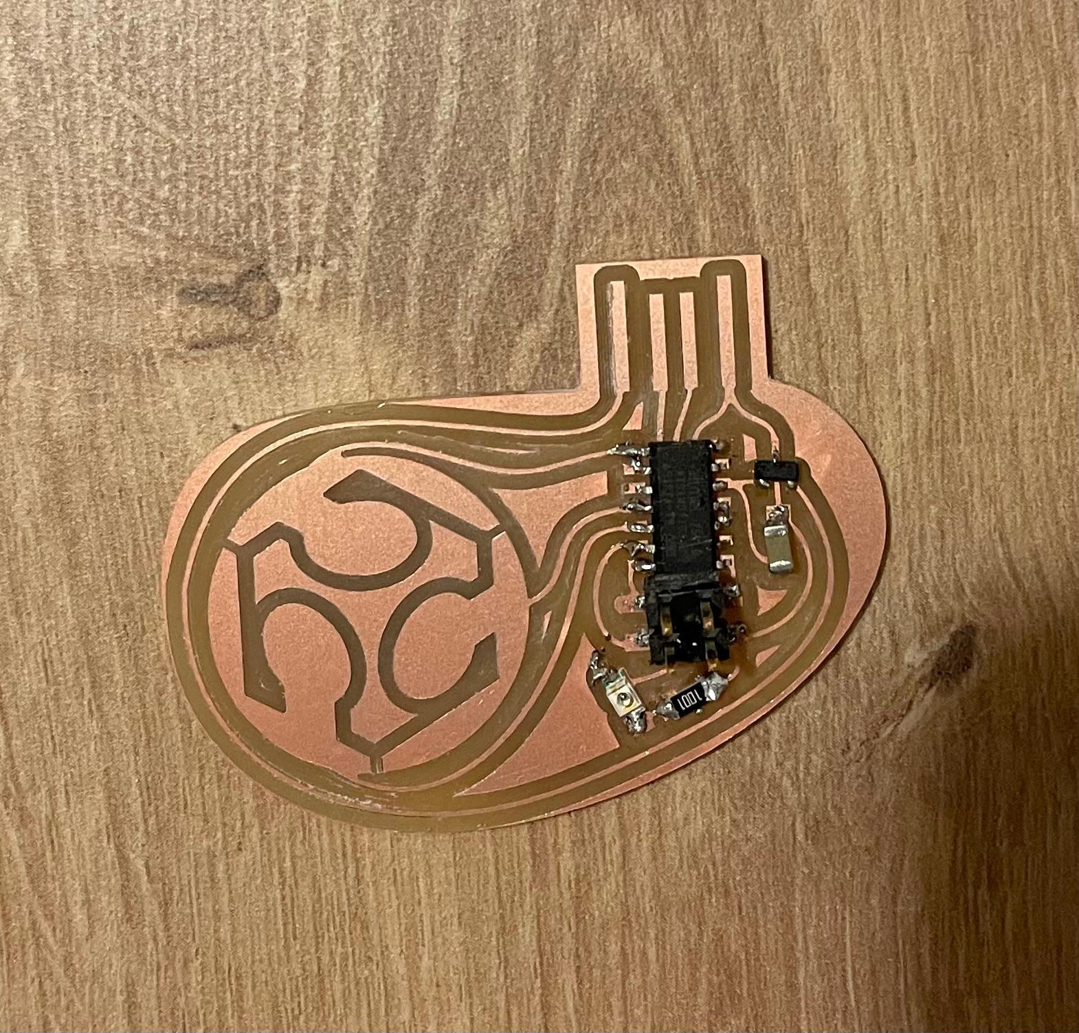
Design your own PCB
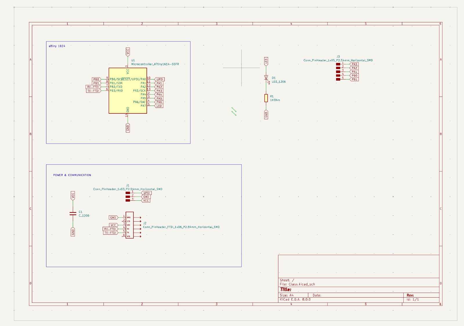
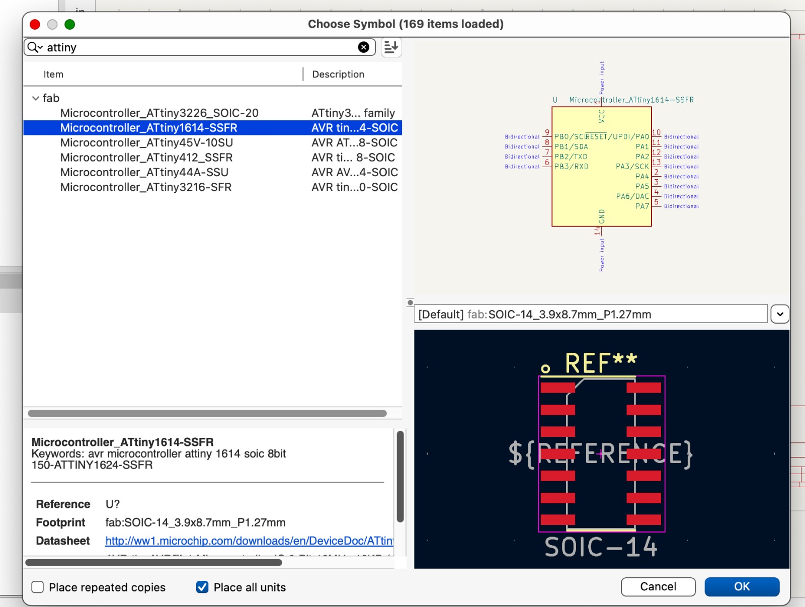
We are building a circuit with ATtiny 1614. First we had to install the program and then add the libraries.
We want to integrate the following elements into the circuit:
- ATtiny 1614
- LED
- Resistor
- Conn_PinHeader (6)
- Conn_PinHeader (5)
- Conn_PinHeader (3)
To be able to connect all elements correctly, we assign labels to the individual elements, so we know where each connection will be. We establish the following labels:
- LED: LED - GND
- RESISTOR: VCC - GND
- Conn_PinHeader (6): VCC, GND, TX, RX, CTS, RTS
- Conn_PinHeader (5): PA3, PA2, PA1, PB0, PB1
- Conn_PinHeader (3): UPDI, VCC, GND
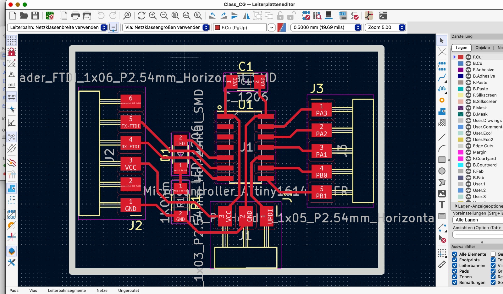
After adding and labeling the elements in the Schematic Editor, we switch to the PCB Layout Editor. All elements are transferred to this layout editor.

We can now arrange the elements so that the traces have the shortest possible paths and do not intersect. Additionally, there must always be sufficient space between the individual traces to ensure that they are isolated from each other. This depends on the width of the traces, which in turn depends on the milling needle thickness we will use. Our drill bit is 0.6 mm thick.
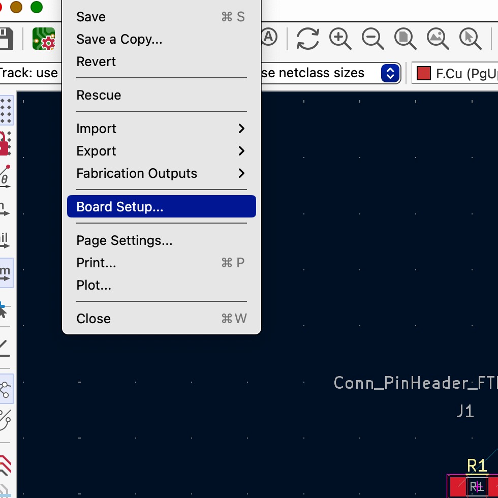
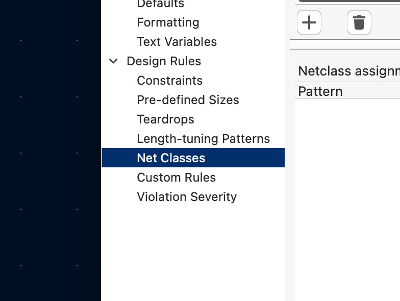
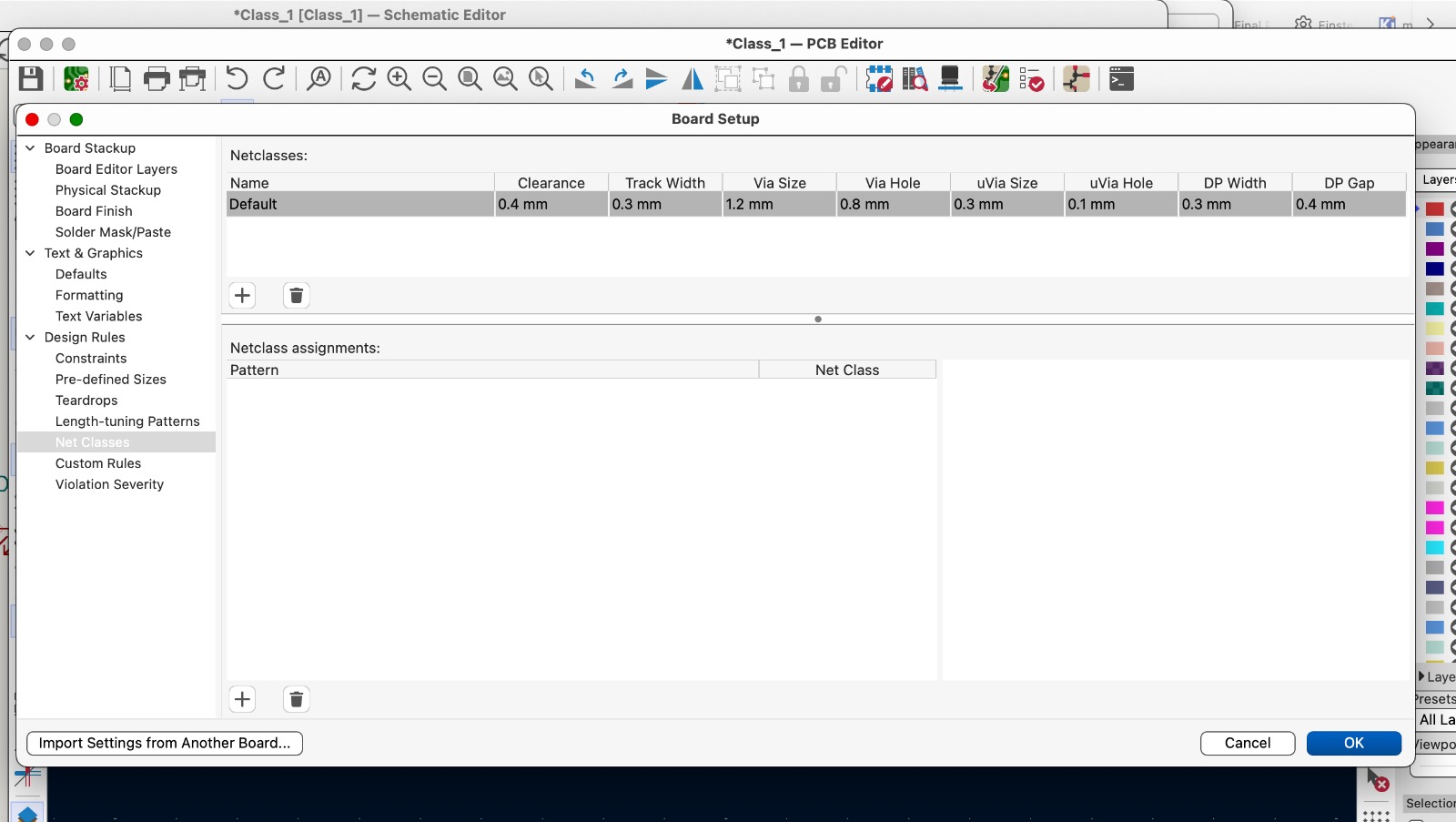
Go to File > Board Setup > Net Classes. This information is important to prevent the traces from overlapping.
- Clearance: Minimum space between traces 0.4
- Track Width: 0.3 mm
- Via Size: 1.2
- Via Hole: 0.8 mm
Now we can start designing. We can also use templates for this. At the beginning, the design may look messy, but the connections are already displayed.
Several shortcuts are helpful for editing in the Schematic or Layout Editor:
- Ctrl + S: Save project
- Ctrl + Z: Undo
- Ctrl + Y: Redo
- Ctrl + C: Copy
- Ctrl + X: Cut
- Ctrl + V: Paste
- R: Rotate
- M: Move without existing wire connection
- D: Move with existing wire connection
- G: Grab traces
When building a circuit, it is always important to know the functions of the individual inputs and outputs:
- TX (Transmit): This pin is used to send data or signals from one device
- RX (Receive): This pin is used to receive data or signals from another device
- Power Supply (VCC): The power supply (often referred to as VCC) provides the electrical energy needed for your circuit to function
- Ground (GND): Ground (or GND) is the reference level for electrical voltages in your circuit
Providing a stable ground connection is important to ensure safe and reliable operation of your circuit. All components and parts in a circuit should be connected to the ground network to ensure a consistent reference potential.
I/O pins are generally used to send and receive signals or data. CTS and RTS are specific control signals that regulate the flow of data in a serial communication link. UPDI: Combines TX and RX.
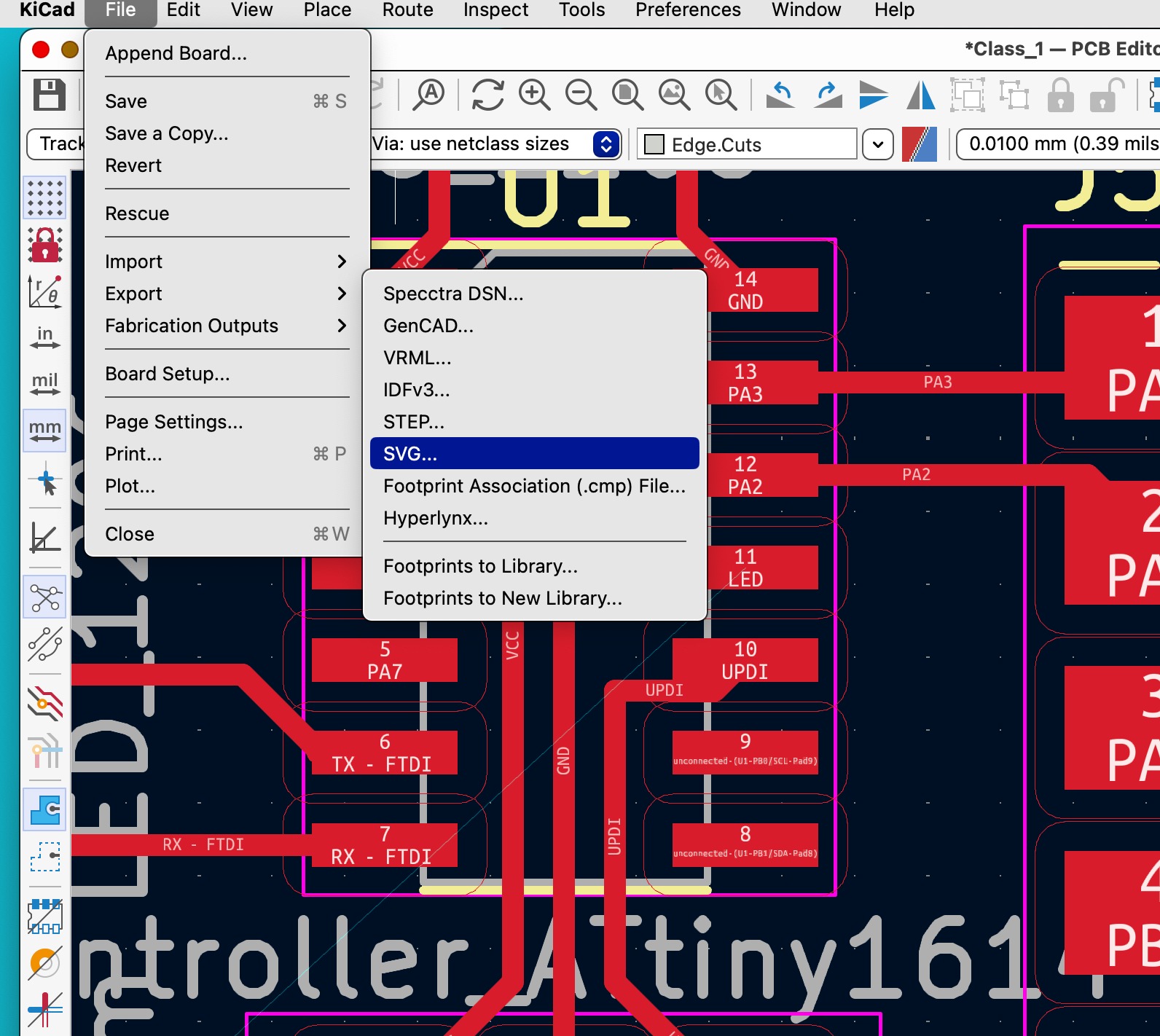
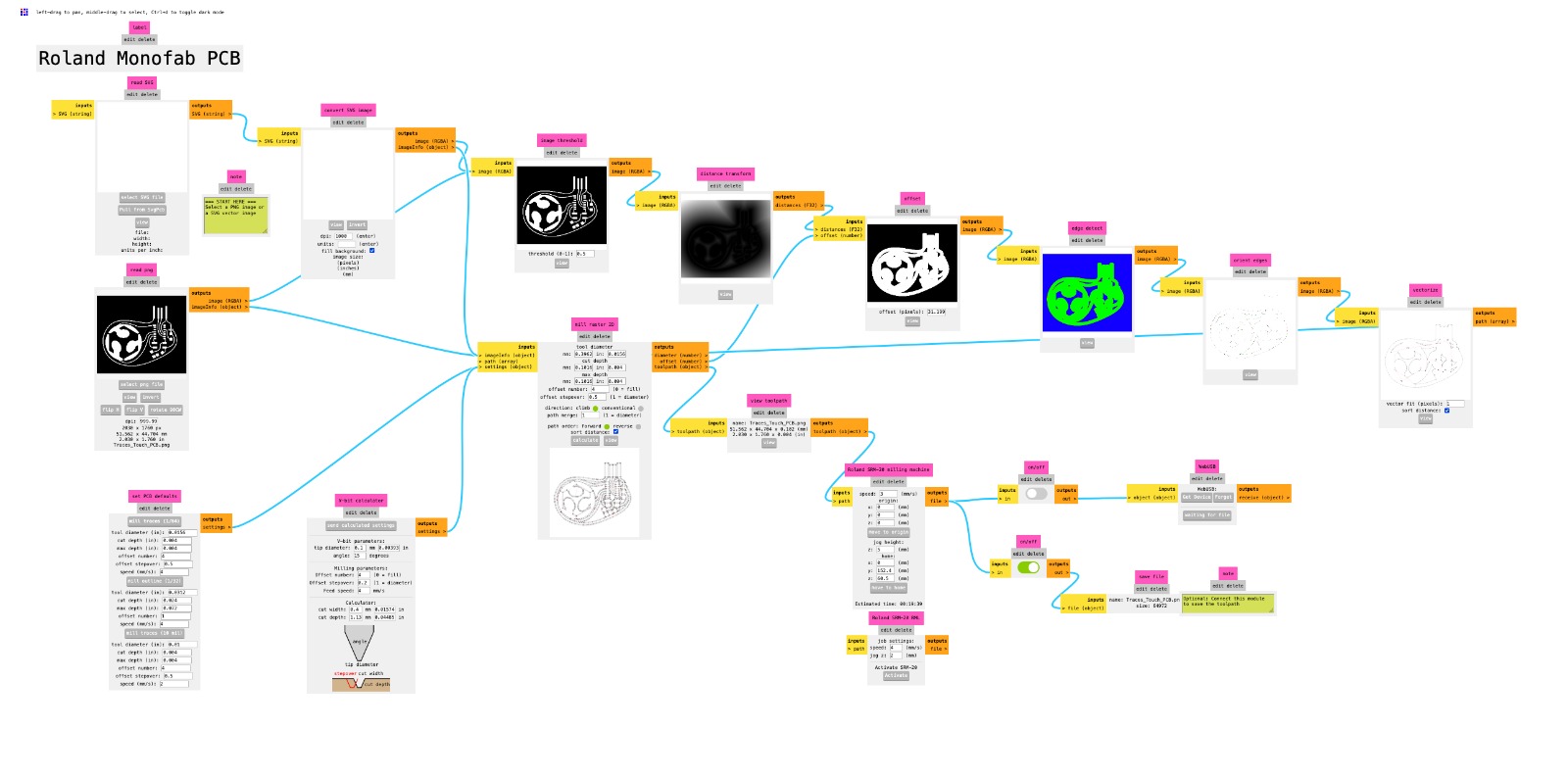
When we have finished a file, we need to open it in Inkscape to make final edits there.
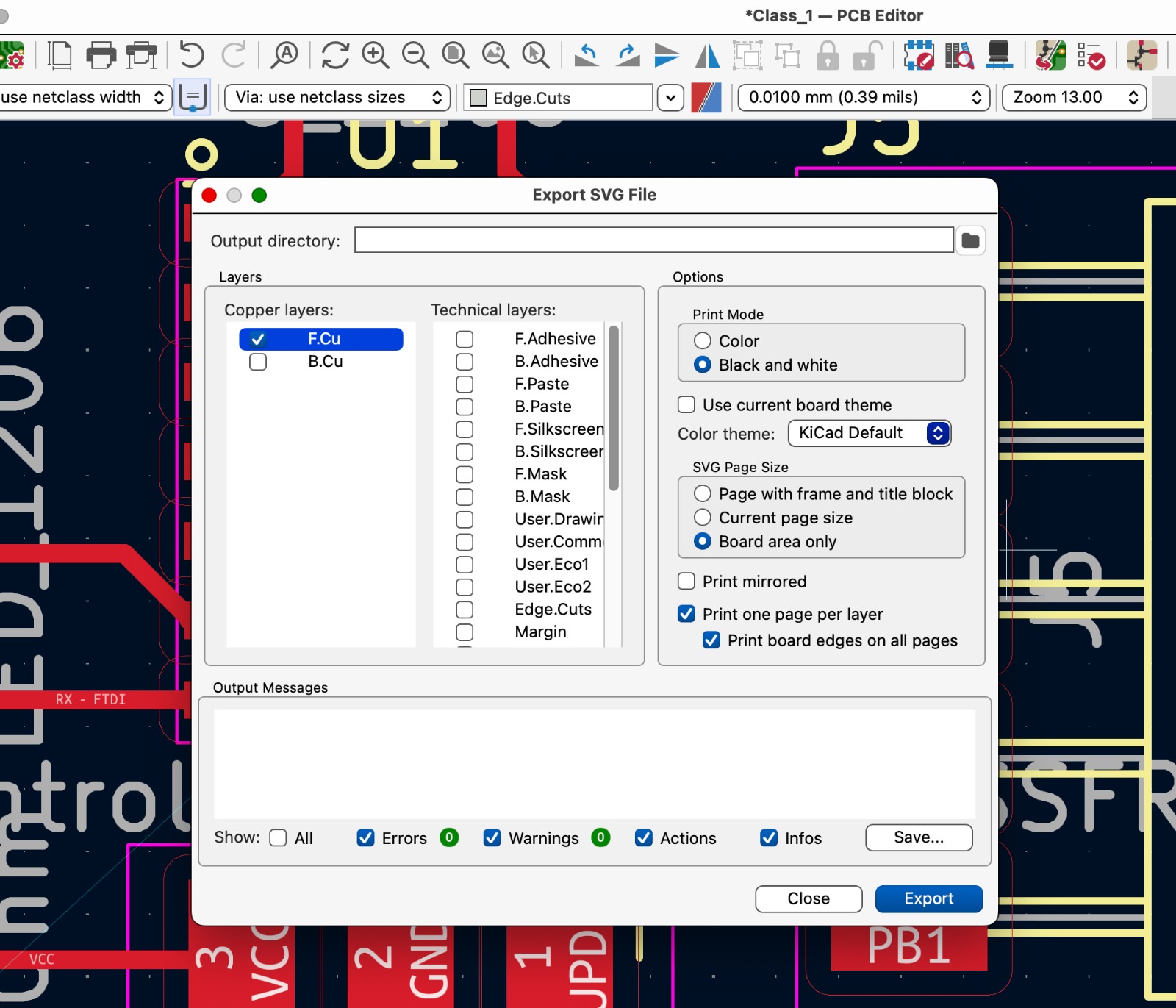
Wir choose Datei > Exportieren > SVG
Wir wählen: F.Cu; Schwarz und Weiß; Nur Platinenfläche; Eine Seite pro Lage drucken, Nur Platinenfläche drucken
Inkscape
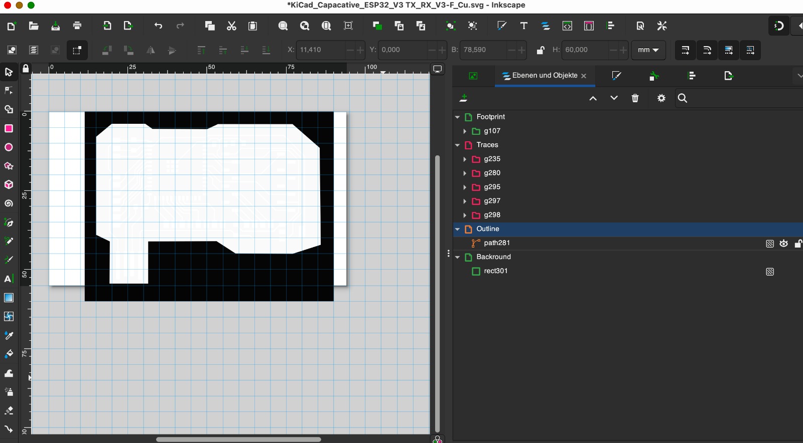
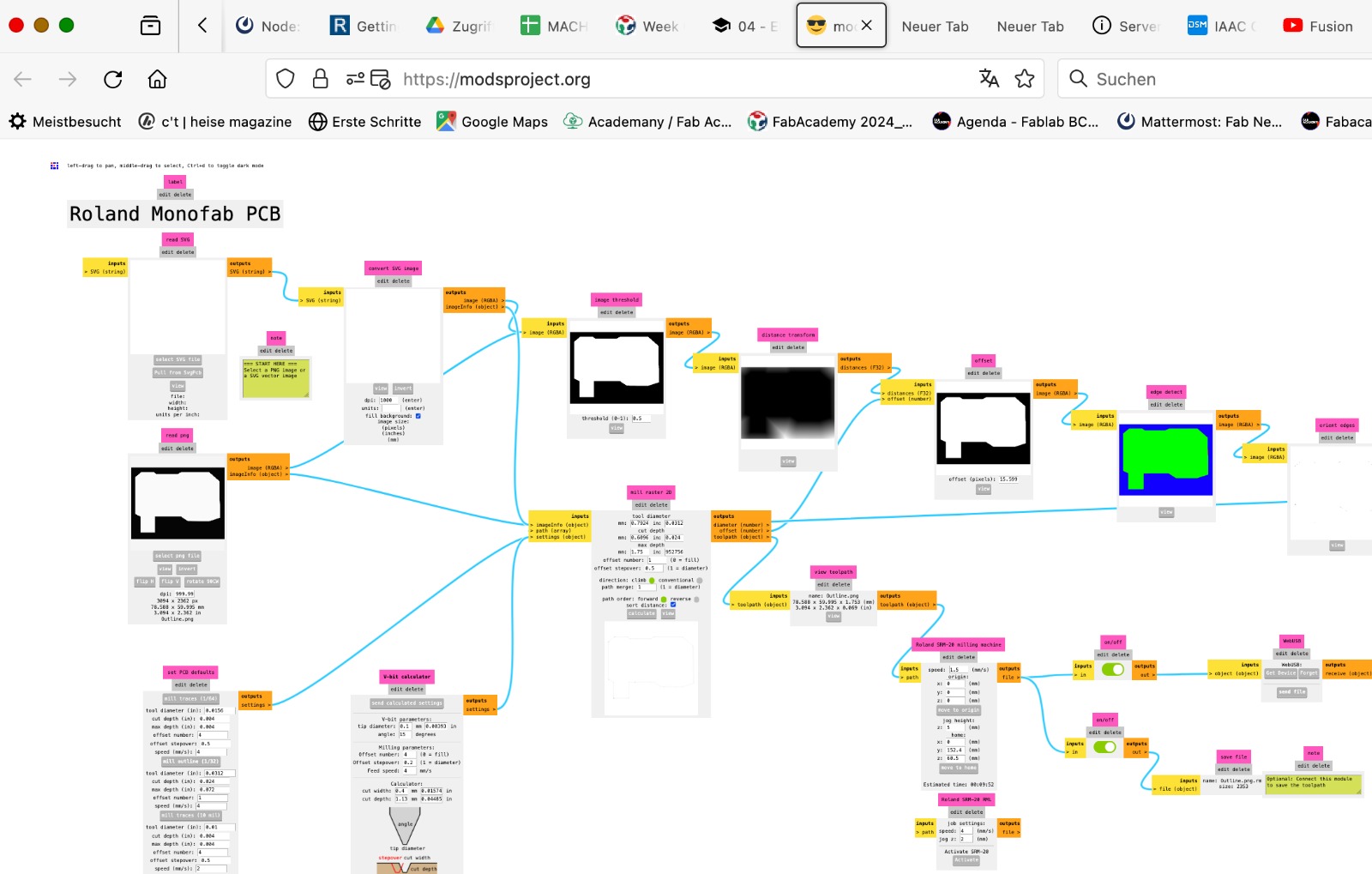
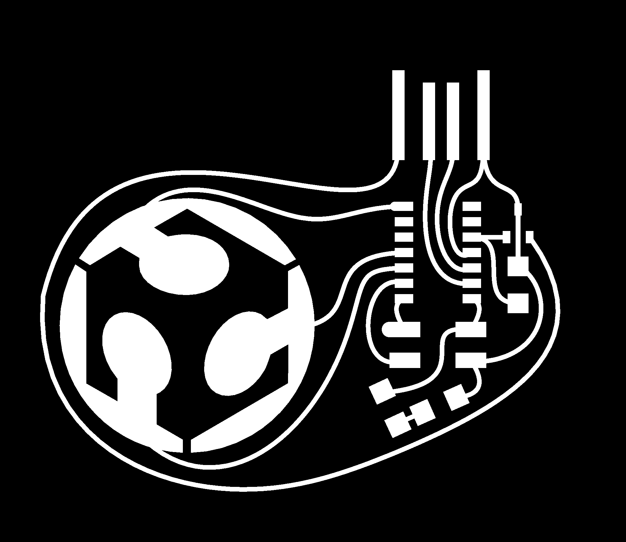
I have to open the file in Inkscape. Tu mill the PCB We need a file for the traces, a file for the outline, and a file for holes. Therefore, we need to assign different layers in Inkscape (Outline, Traces, Holes). I select Layer and Add Layer. I add the layers Traces and Outline. Now, I first select the footprints and traces and move them to the Traces layer by choosing Ebene > Auswahl zur Ebene verschieben > Traces. Then, I select the outline and move it to the Outline layer by choosing Ebene > Auswahl zur Ebene verschieben > Outline.
Now, I can modify the properties of the objects. I first change all the colors of the traces and footprints to white. White is always the color that remains from the milling process, and we want to keep the traces and footprints.
For the outline, I choose a heavy weight, as this is the line I want to cut. Once I have prepared the files, I can export them. I first select the Outline layer.
Export Outline
- Nur Auswahl exportieren (Solo export selected)(in this case I don't choose this)
- DPI: 1000
- Color backround: White (RGB 255, 255, 255)
Than I choose the Layer Traces:
Export Traces
- Nur Auswahl exportieren (Solo export selected) (I select this)
- DPI: 1000
- Color backround: black (RGB 0,0,0)
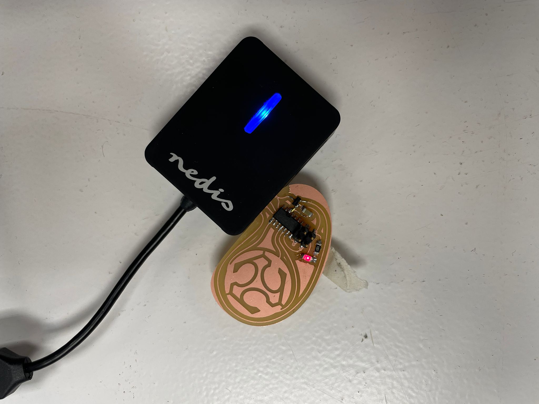
SAMD11
When I had finished the ATtiny, I heard from my fellow students that they hat problemes programming ATtiny with a Mac. Therefore, I decided not to produce it after all. I then decided to make a SAMD11 with a pressure sensor instead. I followed the instructions on the following page and produced the SAMD.
Programming
After the board was complete, I had to make it programmable. I encountered some problems in the process. Since some of my team members were further along than I was, I could use the documentation on their pages and draw on their experience. Moreover, my tutor also assisted me. I carried out the following steps:
To make my SAMD11 board programmable, I had to convert my Quentorres board into a programmer. There is a good explanation on Adrian Torres page
- Download the uf2 file.
- Connect the Quentorres to the PC.
- Use the Boot & Reset function on the Quentorres.
- The PC should now recognize the Quentorres as a USB device so that the uf2 file can be loaded onto it.
Unfortunately, I encountered a problem here that it did not work for me. I had this issue before and knew that it has something to do with my own laptop. To circumvent the error, I uploaded the program on a different laptop. That worked without any problems. The Quentorres then automatically reset, and I could use it as a programmer.
I then proceeded as follows. The procedure can also be found here:
- To make my board programmable, I first had to solder four vertical pins to my Quentorres board.
- I then had to connect the four pins of the new PCB to the Quentorres pins
- I had to open Arduino and paste the following URL under File > Preferences > Additional Board Manager URLs https://raw.githubusercontent.com/qbolsee/ArduinoCore-fab-sam/master/json/package_Fab_SAM_index.json
- Then I had to select Generic D11C14A in the Board Manager
- I also had to select the correct USB port.
- After that, I was able to load the bootloader.
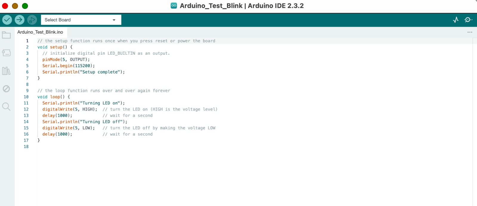
Unfortunately, I also had prolonged problems here, which my tutor initially couldn't solve either. After I did an update of the Arduino IDE, everything worked. As a test, I uploaded the Blink program, and the LED blinked
To make it blink, I just used an example from Arduino. I opened files > examples > basics > blink. I had to define PinMode 31 as an output. To do that, I just changed "LED_BUILTIN" to "31", because the LED is connectet to P31.
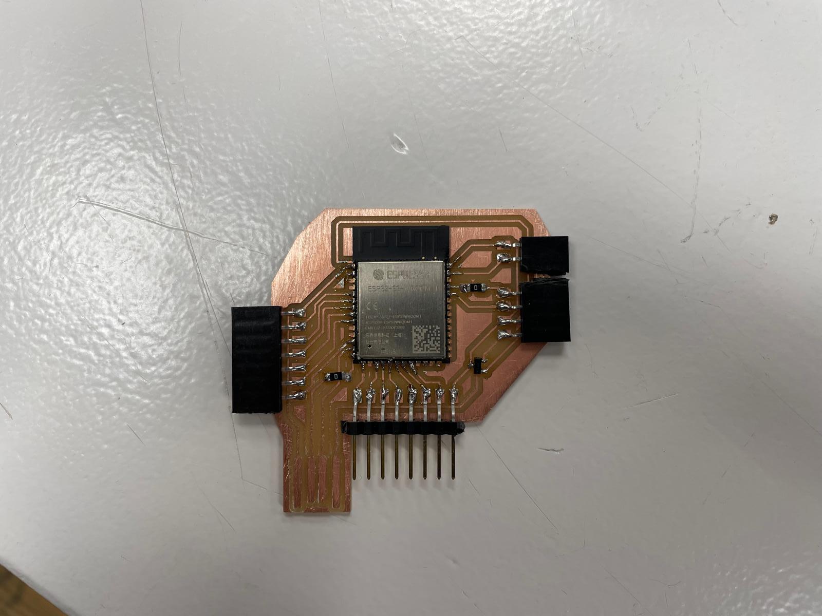
ESP32S3 - Capacitive touch
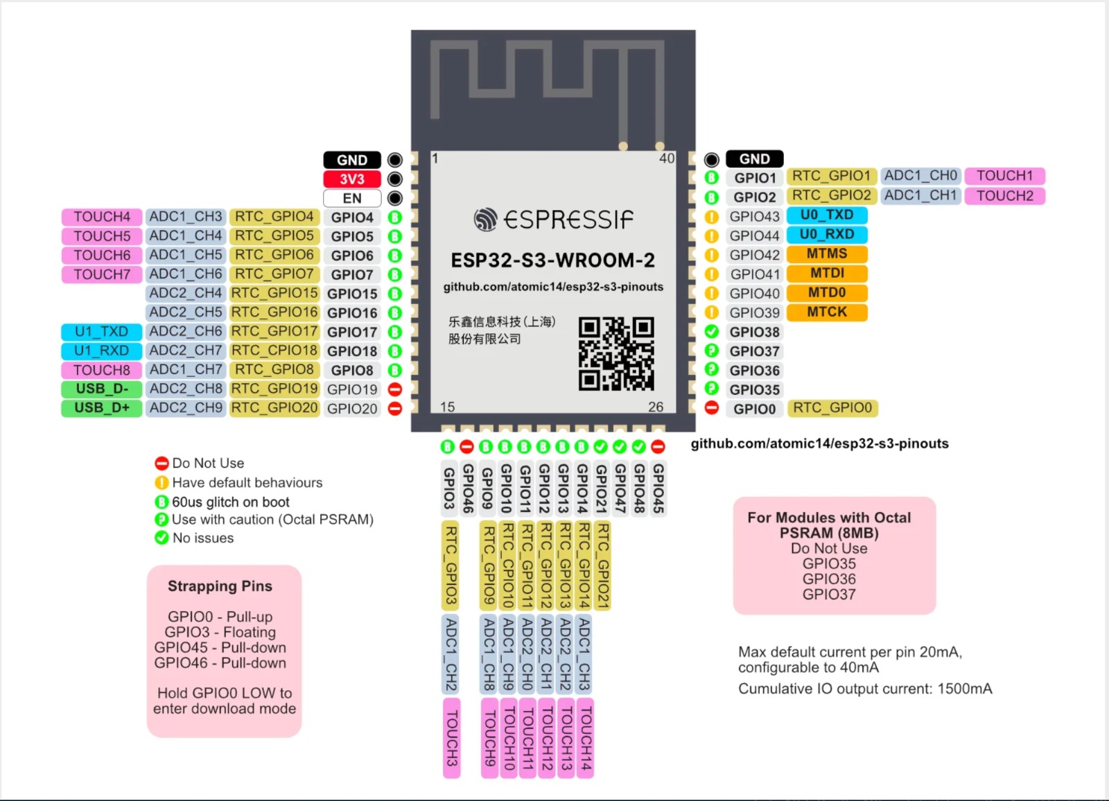 For my final project, I wanted to work with capacitive touch. Since I needed numerous analog touch inputs, I decided on an ESP32S3 board. The board is designed to be linked with 12 different touch fields. At the same time, the board is connected via a TX/RX connection to another board that has an integrated SD card and can connect to two speakers. First, I reviewed the datasheet and pinout to find out which pins could be used as capacitive touch pins, where the TX/RX connection could be established, and where I could integrate an LED.
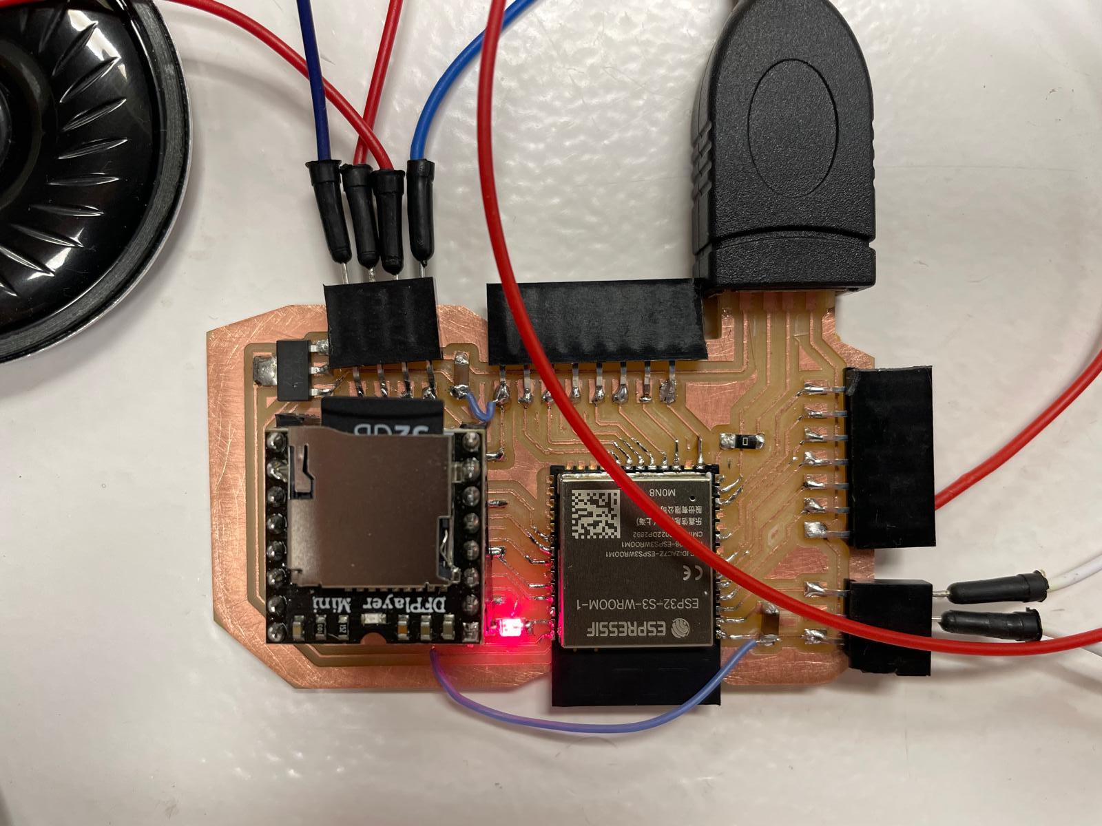
 In my final project, I wanted to connect the ESP32S3 board with the DFPlayer mini to play sounds and songs from an SD card. Initially, I built the board so that the DFPlayer mini was connected via cables through a breadboard. However, my tutor recommended integrating the board directly into the other board.
I used the following pins on the ESP32S3 board:
- Touch IO3 to Touch IO14
- LED
- D+
- D-
- GPIO43 TX
- GPIO44 RX
- 3V3
- EN
- IO
- GND
- Vol-
- Vol+
- Busy
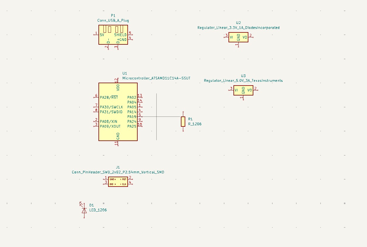
And I needed to integrate the following components:
- Main controller (ESP32-S3-WROOM-1 module)
- Voltage regulator: U1: AMS1117-3.3 (3.3V voltage regulator)
- Resistors: R1: 10 kOhm, R2: 10 kOhm, R3: 330 Ohm
- Capacitors: C1: 10 µF, C2: 10 µF
- Connectors and headers: Various pin headers
- USB connector
- LED: D1: LED (e.g., standard 1206 LED)
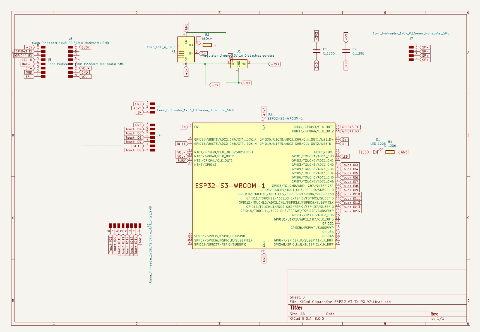
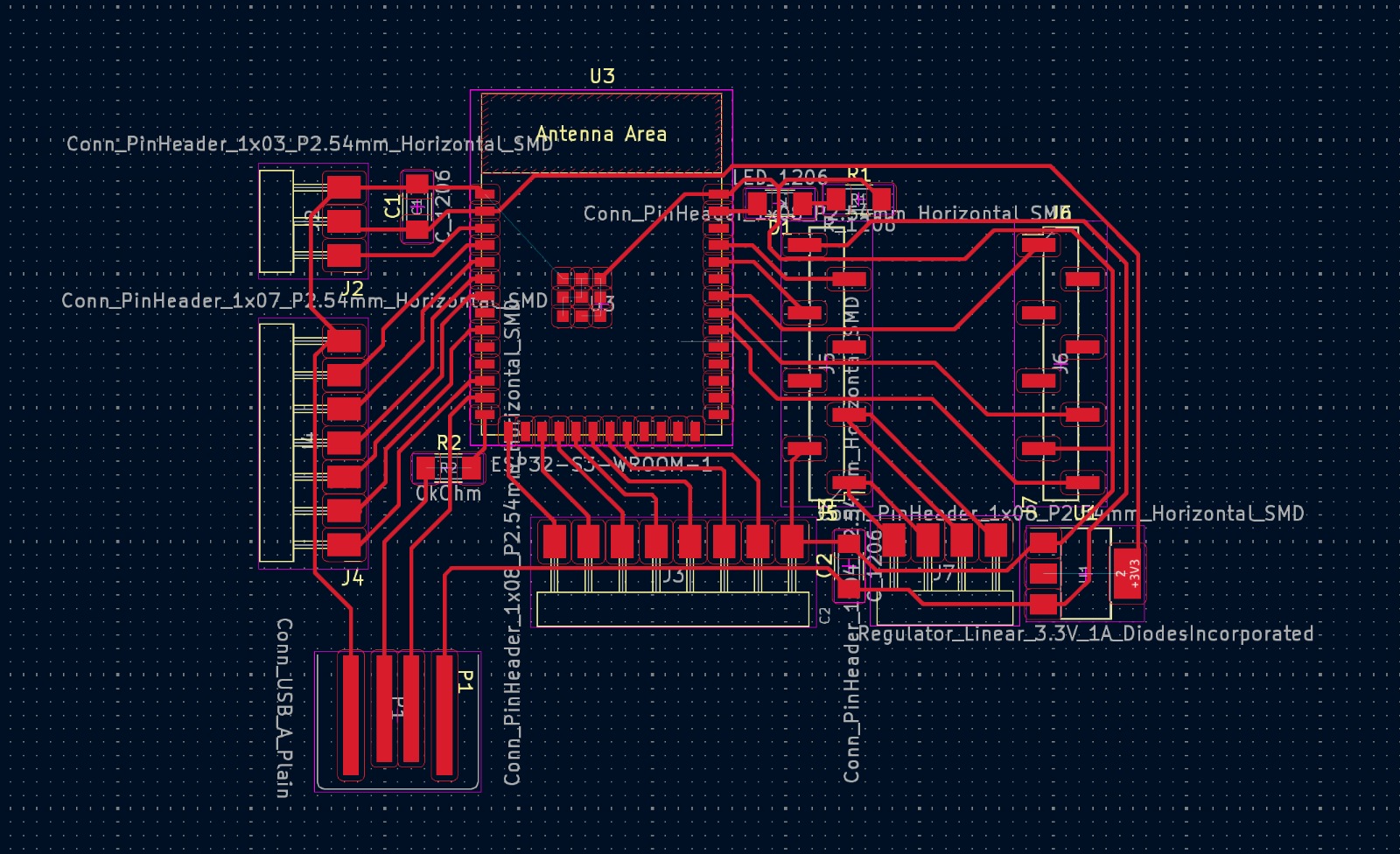
Connecting all the components without crossing the wires was challenging. Regarding the USB connection to the microcontroller, I had to use a 0kOhm resistor to reach the pins. For the PCB design, I used the same presets as in week 8 (Electronics Design): Go to File > Board Setup > Net Classes. This information is important to prevent the traces from overlapping.
- Clearance: Minimum space between traces 0.4 mm
- Track Width: 0.3 mm
- Via Size: 1.2 mm
- Via Hole: 0.8 mm
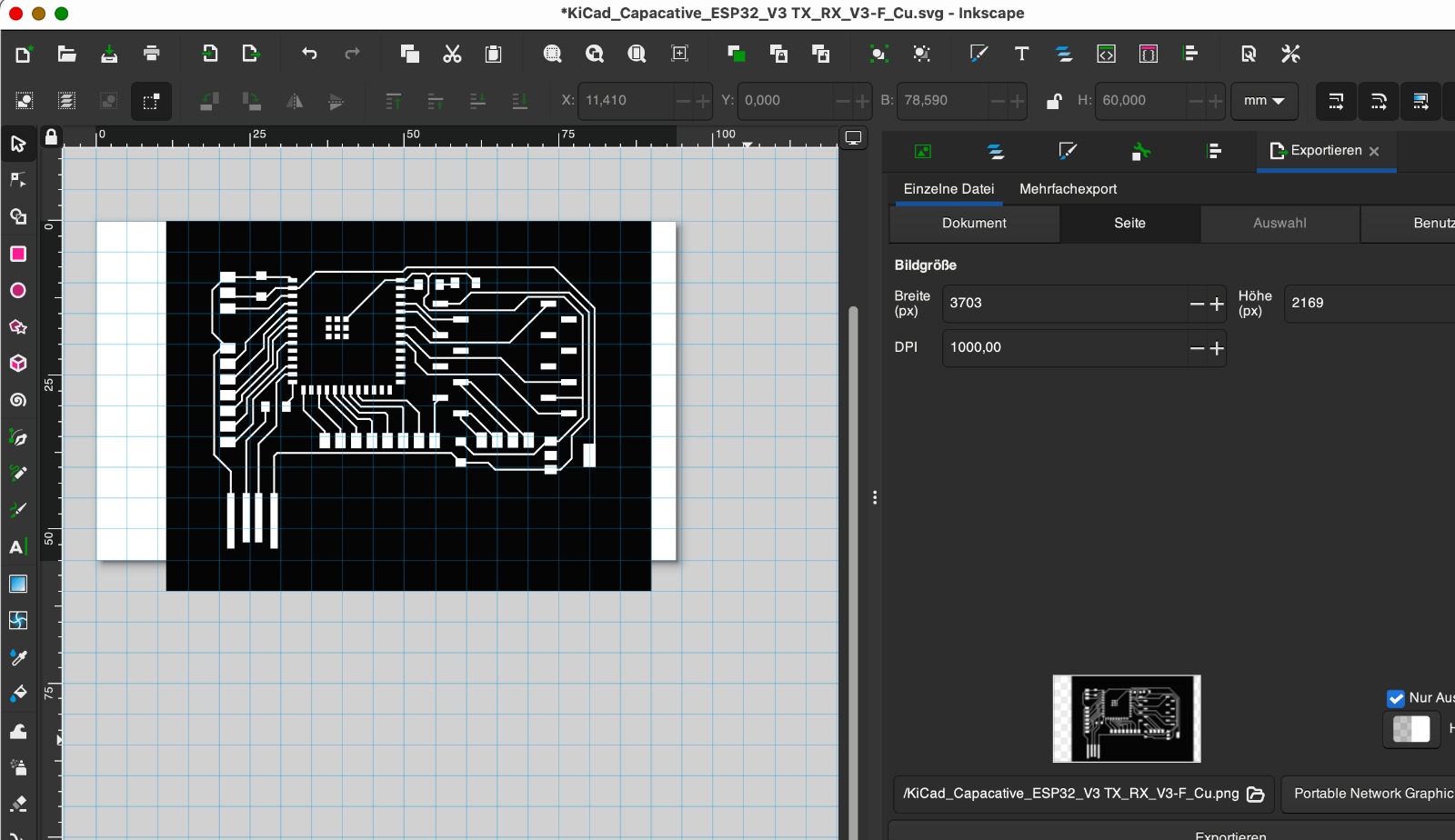
I exported the file and further edited it in Inkscape (as described in week 8). It was important to pay close attention to the size of the USB port outline to ensure it fits well into a USB connector. After adjusting the colors and exporting the high-resolution PNG (for outline and traces), I could begin preparing the files in Mods. I prepared the PNG in Mods as described in week 4.
Milling & Soldering
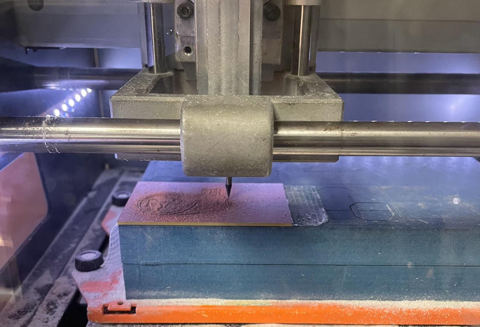
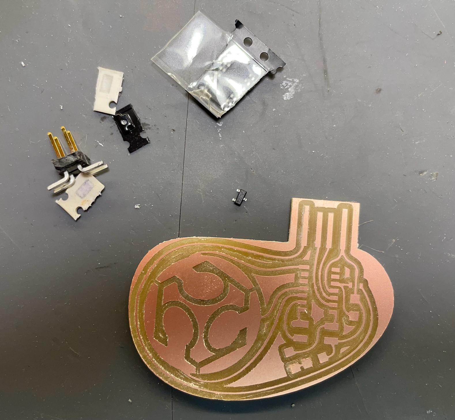
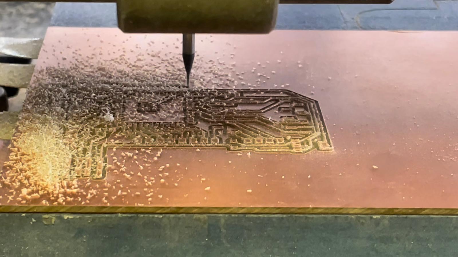
Having gone through the milling process several times, I was already quite familiar with it. However, this time the drill bit broke during the trace cut after about a minute, which was unusual. I flipped the board and, after resetting the zero point, restarted the cut. This time, the board was not milled deeply enough. I asked my tutor to review my file to ensure it wasn't an error in the file. We couldn't find any errors, so we reset the y = 0 point and restarted the cut. Everything worked well. After milling, I had to sand the board as sharp edges had formed. The board looked great afterward, and I could begin soldering. Soldering was challenging because the ESP32S3 has many small pins. After consulting with a classmate, I managed to solder it successfully.
Programming
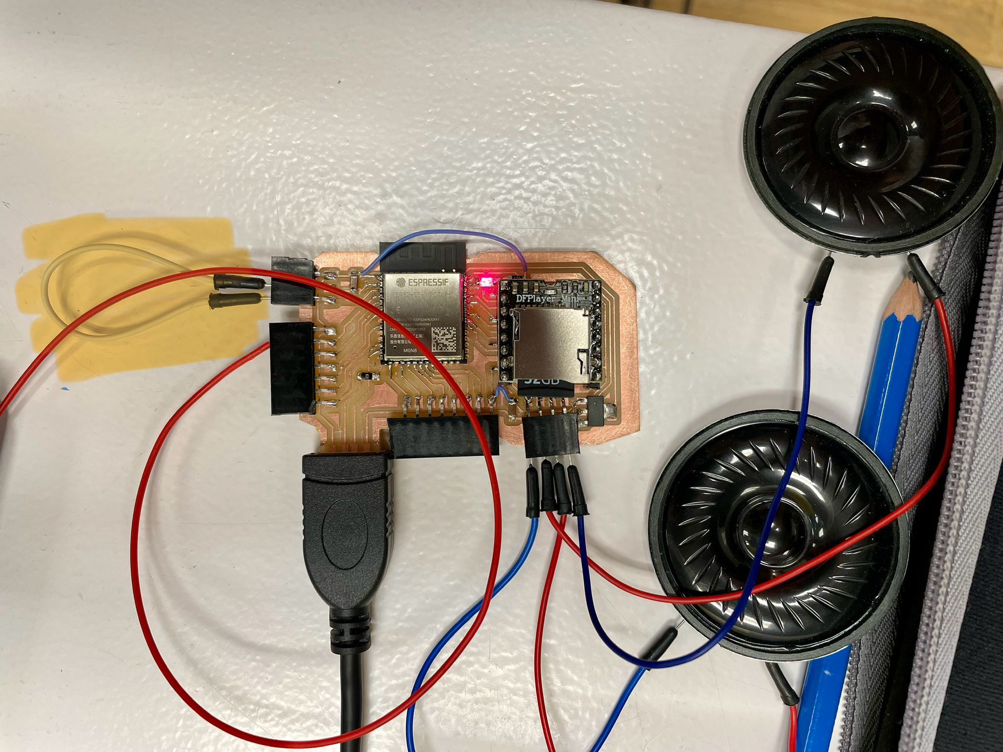 First, I checked if the microcontroller was recognized by the laptop and if I could program it via Arduino. Initially, it didn't work. My tutor helped me, and we found that connecting EN to 3V3 was necessary to establish a stable connection. Once we made this connection, the microcontroller was recognized, and I could upload a simple blink code. To make it work I changed pin 5 (where the LED ist connected) as an Output.
Group assignment
On this page, you will find all the information regarding to our group assignment.